Physical Design
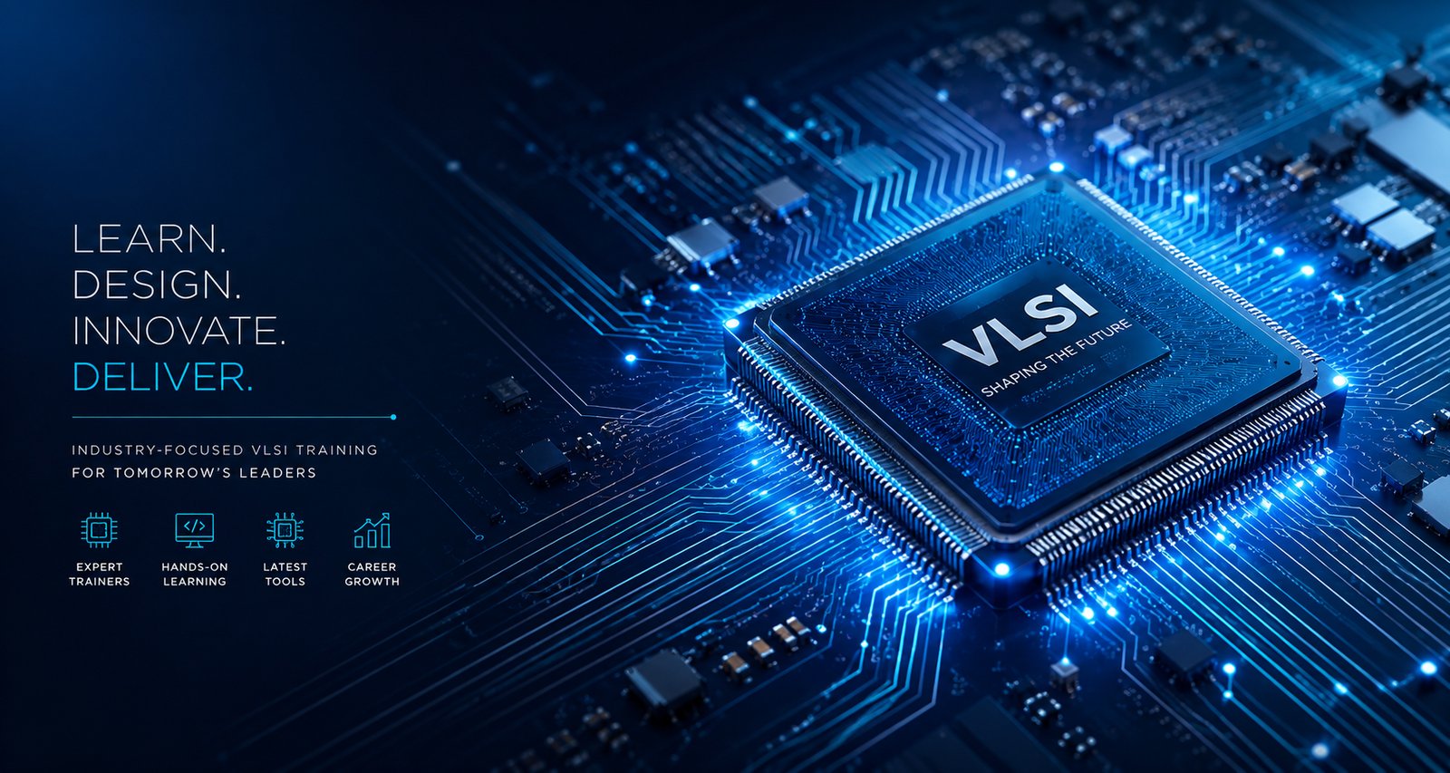
Industry-driven, in-person VLSI training with real EDA tools, expert mentors and placement support — taught by practising engineers in Hyderabad.
Taught by people who've done the job.
Our trainers bring more than 20+ years of combined industry and teaching experience to every session — not just theory, but the judgement that comes from having actually shipped chips.
That translates into a strong, consistent placement record for our students, and a training program that stays closely aligned with what the semiconductor industry is hiring for right now.
20+ years of experience
Combined industry and teaching experience across our training team.
Strong placement record
A consistent track record of placing students into real VLSI roles.
Well connected to industry
Active relationships with hiring partners keep our curriculum current.
Comprehensive VLSI courses
Hands-on curriculum by working VLSI engineers, with real EDA tool exposure and live project training.
Physical Design
Complete RTL-to-GDSII flow covering floorplanning, placement, CTS, routing, timing closure and sign-off on advanced nodes.
Analog Layout
Design and layout of analog ICs including op-amps, ADCs, PLLs and mixed-signal blocks, with FinFET process exposure.
DFT — Design For Test
Scan insertion, ATPG, BIST, boundary scan and test compression strategies used across industry-standard DFT flows.
Design Verification
Functional verification using SystemVerilog and UVM, with constrained-random simulation and formal verification techniques.
Currently only Physical Design admissions are open. Analog Layout, DFT and Design Verification batches will be announced soon.
Technologies you will learn
VLSI is the process of creating ICs by combining millions of transistors on a chip. We train on the exact tools the industry uses — including FinFET nodes like 6nm and 28nm.
Trained by industry. Placed in industry.
Learn from Experienced VLSI Industry Professionals. Our trainers bring real-world semiconductor design experience and practical insights to every session.
Expert industry trainers
Faculty with 10+ years of hands-on experience from leading semiconductor and EDA companies.
Real EDA tool access
Practise on Cadence and Mentor tools — the same software used by companies across the industry.
Placement support
A dedicated placement cell: resume preparation, mock interviews and direct referrals to 15+ hiring partners.
Small batches, personal attention
Limited seats ensure every student gets individual mentoring and guided project work.
Three stages to get admitted
All students must clear all three stages to secure their seat in the program.
Stage 1 — Online entrance exam
Entrance Exam Date will be announced soon. Covers Basic & Digital Electronics, Number Systems, CMOS, BJT, FET and General Aptitude.
Stage 2 — Offline exam
Physical written exam at our Hyderabad centre, on the same syllabus as the online entrance exam.
Stage 3 — Technical interview
A one-on-one technical interview with our faculty panel, for students who clear both exams.
Prerequisites
Engineering background in Electronics or Electrical. Freshers are welcome to apply.
Entrance exam syllabus
Entrance exam
Entrance Exam Date will be announced soon. · online, followed by an offline round on the same syllabus
Batch starts
6 August 2026
Venue
1st Floor, Sreenivasam Building, Image Hospital Lane, Vittal Rao Nagar, Madhapur, Hyderabad – 500081
Everything you need to know
Admissions, fees, training and placements at SeMinds.